Quad Flat No-leads (QFN) Packages

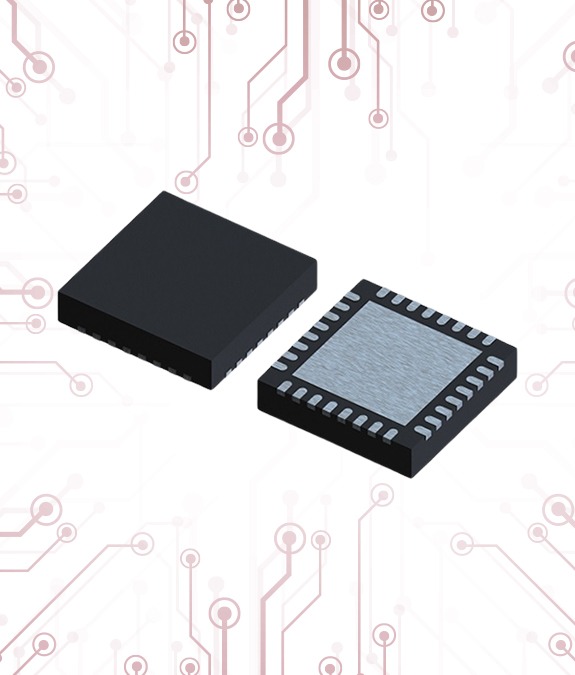
Experience the future of semiconductor packaging with our QFN packages. These surface-mount packages redefine compactness and thermal performance, making them ideal for advanced integrated circuits. The flat, leadless design ensures efficient heat dissipation and ease of manufacturing. Explore the possibilities of QFN packages for your next-generation electronic devices.

The QFN (Quad Flat No-leads) package is a type of surface-mount integrated circuit (IC) package known for its compact size, efficient thermal performance, and versatility. Here are several advantages associated with the QFN package

Advantages of QFN package

Compact Size

QFN packages have a compact footprint, making them ideal for applications with limited board space. This small size allows for high-density packaging on printed circuit boards (PCBs), contributing to the miniaturization of electronic devices.

Low Profile

QFN packages typically have a low profile, allowing for a slim and sleek design in electronic devices. This is advantageous in applications where space constraints and height considerations are critical.

Thermal Performance

The exposed metal pad on the bottom of QFN packages serves as both a thermal and electrical pad. This feature enhances thermal conductivity and allows for efficient heat dissipation, making QFNs suitable for power devices and high-performance applications.

Improved Electrical Performance

The short electrical paths within QFN packages contribute to lower inductance and reduced parasitic effects. This can improve the electrical performance of high-frequency and high-speed applications.

Leadless Design

QFN packages are leadless, eliminating the need for traditional leads or pins. The absence of leads simplifies the manufacturing process, reduces the risk of solder bridging, and contributes to a more reliable connection.

Automated Assembly

QFN packages are well-suited for automated assembly processes, contributing to efficient mass production. The absence of leads simplifies pick-and-place operations, making it easier to handle during assembly.

Ease of Inspection

The leadless design of QFN packages allows for easy visual inspection during the manufacturing process. This facilitates quality control and helps identify any potential issues with solder joints or connections.

Excellent Solder Joint Reliability

The exposed thermal pad on the bottom of the QFN package improves solder joint reliability by providing additional area for solder attachment. This feature enhances mechanical stability and reduces the risk of solder fatigue.

Cost-Effective Manufacturing

QFN packages are often more cost-effective to manufacture than certain traditional packages with leads. The leadless design simplifies the assembly process, reduces material costs, and enhances the overall cost-effectiveness of manufacturing.


Versatility in Applications

QFN packages are used in a wide range of applications, including consumer electronics, telecommunications, automotive, and industrial applications. Their versatility makes them suitable for various types of integrated circuits.

Good High-Frequency Characteristics

QFN packages exhibit good high-frequency characteristics due to their compact design and shorter interconnect paths. This makes them suitable for applications that require high-speed signal processing.

Compatibility with Advanced Technologies

QFN packages are compatible with advanced semiconductor technologies, including the integration of multiple dies in a single package (SiP – System-in-Package) and 3D stacking. This flexibility supports the implementation of cutting-edge innovations.

Discuss your project requirements and experience excellence in semiconductor packaging.