
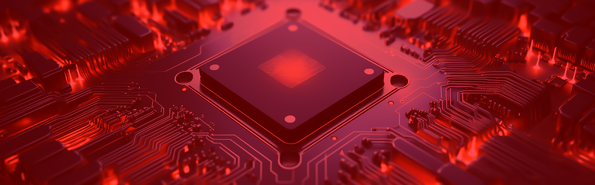
Research & Development
Co-Packaged Optics (CPO): Merging electrical and optical components for unparalleled power efficiency, bandwidth, and latency.
Glass Substrates: Leveraging glass's unique properties for superior thermal management, dimensional stability, and optical clarity in advanced packaging.
Fine Pitch RDL: Achieving ultra-fine routing and high-density interconnect for next-generation electronics.
2.5D and 3D Integration: Combining diverse chips and stacking them vertically to break through planar scaling limitations.
Advanced Heterogeneous Integration: Mastering the art of combining disparate chips for maximum performance and reliability.
Cutting-Edge Interposer Design: Creating high-speed, low-loss connections between electrical and optical domains.
Thin & Ultra-Thin Glass Handling: Enabling compact, lightweight packages with delicate glass substrates.
Next-Generation Optical Chip Technologies: Exploring new materials and architectures for even greater optical performance.
Innovative Glass-to-Chip Bonding: Developing reliable, low-stress attachment techniques for long-term performance.
High-Precision Through-Glass Vias (TGVs): Maximizing integration density with robust electrical and optical interconnects.
Novel Glass-Based System-in-Package (SiP) Architectures: Exploring new packaging paradigms for unprecedented levels of miniaturization and functionality.
Sub-Micron RDL Patterning: Achieving ultra-fine pitch RDL with advanced lithography and etching techniques.
High-Density Through-Silicon Vias (TSVs): Creating reliable vertical interconnects for 3D stacking.
Innovative 2.5D Interposer Technologies: Developing advanced interposers with embedded passives and active components for maximized integration and performance.
Advanced Thermal Management Solutions: Addressing thermal challenges in high-density packages for optimal operating conditions and reliability
Pioneering Co-Packaged Optics: The Future of Integration
At Kaynes Semicon, we’re committed to pushing the boundaries of semiconductor technology. Our dedicated R&D efforts in co-packaged optics (CPO) are paving the way for a new era of integration and performance.
Why Co-Packaged Optics?
As data centers and cloud infrastructures grapple with escalating demands for speed and efficiency, CPO emerges as a transformative solution. By seamlessly merging optical and electrical components, CPO delivers unparalleled benefits:
Unmatched Power Efficiency
Slash power consumption by eliminating the inefficiencies of traditional, separate optical transceivers.
Strategic Lightning-Fast Latency
Experience near-instantaneous communication, crucial for applications demanding real-time responsiveness.
Bandwidth Breakthroughs
Unleash unprecedented data transfer speeds and meet the surging demands of the digital age.
Compact & Scalable
Minimize footprint and enable the construction of denser, more flexible computing architectures.
Our Focus at Kaynes Semicon
We understand that CPO isn’t just a technology, it’s a catalyst for innovation. That’s why our R&D teams relentlessly pursue:
Advanced Heterogeneous Integration
Mastering the art of combining disparate chips seamlessly, maximizing performance and reliability.
Cutting-Edge Interposer Design
Creating the crucial bridges between electrical and optical domains, ensuring high-speed, low-loss connections.
Next-Generation Optical Chip Technologies
Exploring new materials and architectures to unlock even greater optical performance.
Partnering for Progress
We believe in collaboration. We’re actively seeking partnerships with industry leaders, research institutions, and innovators to accelerate the adoption of CPO and shape the future of interconnected systems.
Join the CPO Revolution
At Kaynes Semicon, we’re not just developing technology, we’re envisioning a future where data moves at the speed of light. If you share our passion for pushing boundaries, get in touch. Let’s build the future together.

Glass Substrates: Redefining Packaging Possibilities
In the world of advanced packaging, where miniaturization and performance are paramount, glass substrates are emerging as a transformative solution. At Kaynes Semicon, we’re harnessing the unique properties of glass to unlock new dimensions in packaging technology.
Why Glass Substrates?
Traditional packaging materials often struggle to meet the demands of next-generation electronics. Glass, with its inherent advantages, is rewriting the rules:
Superior Thermal Management
Dissipate heat efficiently, enabling higher power densities and improved reliability.
Exceptional Optical Clarity
Ideal for applications leveraging photonics, from high-speed communication to biosensors.
Unmatched Dimensional Stability
Maintain precision form factors, even under extreme temperatures, crucial for complex 3D integration.
Chemical & Environmental Resilience
Resist corrosion and withstand harsh conditions, ensuring longevity and performance
Thin & Ultra-Thin Glass Handling
Mastering the art of working with delicate glass substrates, enabling compact, lightweight packages.
Innovative Glass-to-Chip Bonding
Developing reliable, low-stress attachment techniques, ensuring long-term performance.
High-Precision Through-Glass Vias (TGVs)
Creating robust electrical and optical interconnects, maximizing integration density.
Novel Glass-Based System-in-Package (SiP) Architectures
Exploring new packaging paradigms, enabling unprecedented levels of miniaturization and functionality.
Our R&D Focus at Kaynes Semicon
We’re not just adopting glass, we’re pushing its limits
Our R&D Focus at Kaynes Semicon
We’re not just adopting glass, we’re pushing its limits
Thin & Ultra-Thin Glass Handling
Mastering the art of working with delicate glass substrates, enabling compact, lightweight packages.
High-Precision Through-Glass Vias (TGVs)
Creating robust electrical and optical interconnects, maximizing integration density.
Innovative Glass-to-Chip Bonding
Developing reliable, low-stress attachment techniques, ensuring long-term performance.
Novel Glass-Based System-in-Package (SiP) Architectures
Exploring new packaging paradigms, enabling unprecedented levels of miniaturization and functionality.
Pioneering a Glass-Enabled Future
We see glass as more than a material, it’s a gateway to innovation. By combining our expertise in semiconductor manufacturing with cutting-edge glass technologies, we’re envisioning a future where packaging constraints are a thing of the past.
Collaborate with Us
We’re eager to partner with visionaries across industries to explore the limitless possibilities of glass substrates. If you’re ready to challenge the status quo and redefine what’s possible in packaging, let’s connect. Together, we’ll turn glass into gold.
Fine Pitch RDL, 2.5D, and 3D: Connecting the Future of Integration
At Kaynes Semicon, we’re at the forefront of advanced packaging technologies. Our expertise in Fine Pitch Redistribution Layer (RDL), 2.5D, and 3D integration is enabling a new era of high-performance, densely packed electronics.
Why Fine Pitch RDL?
As semiconductor devices shrink and I/O counts skyrocket, traditional interconnect methods face limitations. Fine Pitch RDL offers a crucial solution:
Unparalleled Density
Achieve ultra-fine routing with line widths and spaces approaching the limits of lithography, maximizing interconnect density.
Superior Signal Integrity
Minimize crosstalk and ensure pristine signal transmission, even at high frequencies, essential for advanced applications.
Enhanced Flexibility
Enable complex fan-out patterns and accommodate diverse chip architectures, facilitating seamless integration.
2.5D and 3D Integration: Breaking the Barriers
When planar scaling reaches its limits, we turn to the third dimension. Our 2.5D and 3D integration capabilities unlock new possibilities:
Heterogeneous Integration
Combine diverse chips – logic, memory, sensors, and more – into a single package, achieving unprecedented performance and functionality.
Reduced Form Factor
Stack chips vertically, minimizing footprint and enabling compact, powerful devices.
Improved Power Efficiency
Shorten interconnect distances, reducing power consumption and enhancing overall system performance.
Building a More Connected World
We believe that Fine Pitch RDL, 2.5D, and 3D integration are key enablers of next-generation electronics. From AI and high-performance computing to mobile devices and automotive systems, our technologies are powering innovation across industries.
Partner with Us
We’re committed to collaborating with industry leaders, research institutions, and forward-thinking companies to shape the future of interconnected systems. If you’re ready to embrace the possibilities of advanced packaging, let’s connect. Together, we’ll build a more connected, intelligent, and efficient world.